[CDNS – Cadence; SNPS – Synopsys] The evolution of the EDA industry

It used to be that a chip engineer would design an integrated circuit by hand drawing a few dozen pages of schematics using standard templates, the resulting patterns X-ACTO knifed out of plastic film. But with transistor density doubling every 18 months, this manual process couldn’t scale and was eventually replaced with a technology called logic synthesis, where engineers specify in a high level programming language1 what they want their chip to do and those instructions are synthesized into a list (“netlist”) of cells (groups of transistors2) and connections that together perform logical functions.
That netlist is then run through various test programs to ensure that the chip’s billions of transistors turn on and off in certain configurations at precise times according to certain rules, before then being converted to an algorithmically generated blueprint delineating where cells are laid out on a chip and how those cells should be wired together (a process called “place and route”). Then, in the sign-off stage a bunch more tests are run to ensure that the place and route layout matches the original circuit design schematic, that the IC works as intended under simulated workloads, and that the huge number of design rule checks (DRC) of the fab that will manufacturer the chip have been followed.
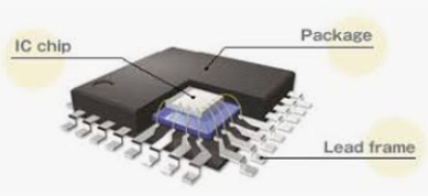
The fab then turns the design into a physical stencil, through which it shoots light to imprint the stencil pattern onto the dies (integrated circuit chips) that make up a coated silicon wafer. Those chips are secured to a plastic or ceramic package and hooked up to thin gold filaments that transport electricity in and out of the chip.
Obviously, what I’ve just described obscures loads of detail. Even with sophisticated Electronic Design Automation (EDA) software from Synopsys and Cadence, it can take hundreds of engineers and months of laborious work to design an integrated circuit. The design flow, from synthesis to sign-off, is incredibly ornate and gets ever more so as process nodes3 get smaller and smaller.
And with the cost of chip design rising alongside smaller geometries – exploding from just $150mn when the industry was on a 10nm process node to over $500mn on 5nm – the consequences of taping out development errors can be devastating.

[Whereas 5-10 years ago, designers might spend 5 months building a chip and another month programming it with software, today each step takes around the same amount of time. And so, to keep chip design moving along at the same rate, software development must begin ~3-4 months earlier, before the hardware has been completed. This dynamic has created a significant tailwind for Synopsys’ emulation device, which allows designers to create a virtual model of the hardware on which to write the software]
EDA engines evolved to meet mounting design complexities and, with OEMs under constant pressure to meet the insatiable demand for more speed and power efficiency as quickly as possible, have compressed the design process to hasten time-to-market. For instance, a decade ago, Synopsys started combining parts of the validation stage into place-and-route. A few years after that, it launched a solution that simultaneously verified chips and the embedded software running on the chips, shaving 6 to 9 months off the development cycle. The company’s latest platform, Fusion, released after 5 years of development, “fuses” various tools that address the three phases of design – synthesis, place-and-route, and sign-off – so that they all share a common data model, allowing a designer can more easily move back and forth between them.