Cadence, Synopsys, and the Future of Chip Design

As a reminder, I’ll be in Omaha hanging out on the 2nd Floor of Upstream this Friday, around 8pm. If you’re around, please swing by!
Related posts:
[CDNS – Cadence; SNPS – Synopsys] The evolution of the EDA industry (2/28/20)
Simulation, CAD, and PLM: Part 1 (7/30/20)
I.
I’ve always found it conceptually helpful to think of a digital chip as a city, with buildings, roads, and the bustle of people mapping to IP blocks, wires, and the flow of electrons. Plus, look. A system-on-chip schematic sort of looks like a city viewed from above:
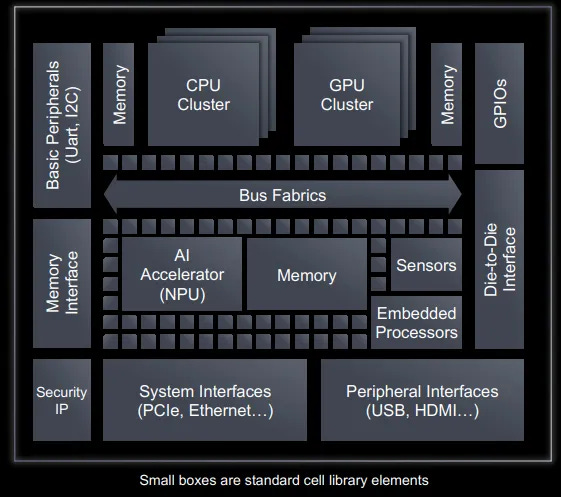
Source: Synopsys Analyst Day (3/20/24)
(aside: the following discussion pertains to digital chip design, a market that is roughly 4 or 5 times larger than analog. Analog chip design is similar to digital chip design in that in involves laying out circuits and running simulations to test performance, but it is far less automated and doesn’t make use of as much high level descriptive languages. A more detailed description of analog design can be found here)
Just as an urban planner might begin with a vision of what they want a city to be – a bustling environment powered by commerce that preserves a sense of community – before considering the particulars of what it looks like, so too does a chip designer start with high-level intent, the actions performed in different states. This is expressed at the Register-Transfer Level (RTL), where the engineer describes – using a hardware description language like Verilog or VHDL – how data is transformed by logic operations and transferred between registers at defined time intervals (i.e. at each clock cycle). Their code might specify something like: “on every clock cycle, perform an AND operation on this data, then move the result from register B to register C.” (registers, in this context, are small memory cells within the processor that temporarily hold values being actively manipulated).
After the RTL is written, it undergoes a process called functional verification, where the design is exhaustively tested to ensure it behaves exactly as intended. For example, if a CPU is instructed to add 2 and 2, it should return 4 under a wide range of edge cases and simulated stress scenarios. Functional verification is essential because it allows designers to catch logic errors early, while the chip is still an abstract model written in code, well before that code is turned into a costly, immutable physical layout. It is also widely considered the most time-intensive step, often consuming up to 40% of chip development time. Of the ~40 or 50 tools used from design start to finish, ~10 are concentrated here. In fact, functional verification is so resource-intensive that it’s often treated as its own distinct category within chip design.…as in, there’s verification and then there’s everything else, and the number of engineers working on everything else is like a third of the number working on verification, as different engineers are responsible for testing different RTL blocks separately, before those blocks are tested in combination1. Once functional verification is complete, RTL is converted to lower, machine level logical representations (logic synthesis), the output of which is a netlist that details how the cells on a chip that perform logic operations connect to one another, as well as the power and timing specs of those cells.
So, that’s the front-end of design. The back-end is where the front-end’s textual representations are converted to geometry. It starts with floorplanning, where components (CPU cores, USB interfaces, memory blocks, etc.) are organized on a virtual die. This is a hierarchical process where sub-blocks are individually optimized before being integrated into a larger whole. For instance, in a CPU, standard cells like logic gates, flip-flops (the building blocks of registers), and other components are combined into CPU cores, those cores are combined into clusters, those clusters are merged into a higher-level system that includes other functional subsystems – memory, graphical processing, security, multimedia – that were also built bottoms-up from constituent blocks, all with timing and power considerations in mind. Those subsystems are iteratively arranged to reduce the lengths of interconnects (wires connecting blocks and subsystems)2, minimize power consumption, and ensure that the clock signals that trigger operations (fetch data, execute logic, etc.) reach the right components at the right time.
The high-level blueprint created during floorplanning – which defines where major functional blocks will reside on the chip – is translated into fine-grained detail during place and route (P&R). Working within the spatial and connectivity constraints set by floorplanning, the P&R tool places logic gates close to associated flip-flops to minimize signal travel time. Buffers are inserted along clock paths to ensure signals arrive at different components in sync. Meanwhile, interconnect wires between gates, blocks, and subsystems are routed to reduce latency, avoid congestion, and minimize electrical interference (crosstalk) from adjacent wires.
P&R is then followed by Parasitic Extraction, where unwanted delays and electrical effects are identified3. What follows are a series of checks to verify that:
1) data arrives exactly when it’s supposed to (Static Timing Analysis) and signals are free of noise and interference (Signal Integrity Checks);
2) the physical design conforms with a fab’s manufacturing rules, like that the wires are of such-and-such width and spaced at such-and-such distance (Design Rule Checking, or DRC);
and,
3) the layout is functionally identical to netlist synthesized earlier, with no missing or redundant transistors or connections (Layout vs. Schematic, or LVS).
Once this sign-off process is complete, the finalized layout is delivered to the fab in a GDSII or OASIS file format. The foundry then uses this file to create the photomasks needed for manufacturing, a milestone known as tape-out.
Returning to the earlier city analogy, the front-end of chip design is like planning a city: defining zoning guidelines, permitted activities and structures, and specifying how buildings should connect to roads and utilities. The back-end, by contrast, is akin to actual construction. Floorplanning maps out where major roads, districts, and buildings should go, while place and route (P&R) fills in the fine details – laying down building components, wiring up network cables, installing power lines, and coordinating traffic lights. Finally, the sign-off process resembles the work of a city inspector, certifying that all streets, utilities, and structures meet regulations and faithfully match the original plans.
II.
If this is a city, it is an extremely centrally planned one, where every building, sidewalk, and power line is specified in advance, and every person is expected to show up to a designated place at exactly the right time. But control becomes harder to achieve as every component and connection is shrunk down in size. As transistors get smaller, quantum effects begin to intrude. Gates that block or allow the movement of electrons across a tiny channel – from the “source” where electrons originate to the “drain” that collects electrons on the other side – stop closing all the way and some electrons even tunnel through channel barriers (you might analogize the source to a water faucet, the electrons to the water that pours out of the faucet, the drain to the sink the water dumps into, and the gate as the faucet valve that controls the flow of water). Even when a transistor is supposed to be idle, some electrical current leaks through anyway, consuming power and generating heat. Smaller nodes also require thinner wires bunched more closely together, producing signaling delays and noise from higher resistance and capacitance (see footnotes). In short, as transistors shrink beyond a certain size, the gate’s ability to control the electric current across the channel deteriorates (the water faucet’s valves don’t turn on or shut off the flow of water as well as they should).
These issues began to surface sometime around the mid-2000s. Up to then, as predicted by Moore’s Law and Dennard scaling, transistor density was doubling every ~2 years while power density remained constant, yielding chips that were faster and cheaper and more energy efficient. This worked because the voltage required to switch a transistor on and off decreased along with transistor size, allowing more transistors to be packed into a given area without increasing total power consumption. However, below a certain size, voltage scaling breaks down: further reductions increase power density, generate more heat, worsen current leakage, and raise the risk of logic failures and timing violations. No more free lunch! To keep the chip operating in a safe temperature range, clock speeds are reduced or functional blocks on a chip are powered down, degrading performance and increasing per unit compute cost.
The performance-atrophying effects of lower clock speeds can be mitigated by distributing workloads across more processing cores, with each core working in parallel. But this comes with its own issues. As transistors shrink and more cores are added, the interconnects linking them become thinner and must span longer distances, increasing resistance, degrading signal quality, and consuming more power. Also, cores compete for access to shared memory, and memory bandwidth doesn’t scale linearly with core count.